3rd International Conference on
Optics and Laser Technology
October 29-30, 2026 | Berlin, Germany

Address: Hans-Grade-Allee 5, 12529 Schönefeld b. Berlin, Germany
Optics 2026

Ernst-Abbe-University of Applied Sciences Jena, Germany
Abstract:
This article examines
the potential and possibilities of a new laser-based process (LSA) for the
selective metallization of three-dimensional circuit carriers. The polymer
substrates can be used without additional metal fillers in the matrix, thus
saving costs and resources. The area of application extends to injection-molded
and additively manufactured plastic components. The process is divided into the
process steps: surface activation due to laser structuring (1), nucleation of
palladium on these surfaces (2) and electroless copper plating of the activated
areas (3). Experimental investigations with three pulse duration from
nanoseconds to femtoseconds are presented. These differ in the selected laser
and pulse parameters. By varying significant process variables, interaction
processes are analyzed which have a decisive influence on the subsequent activation,
nucleation and metallization. The focus is on discussing the influencing
parameters for generating partially conductive structures. As a result,
exemplary process windows for polybutylene terephthalate and polyamide are
shown. The important target values electrical resistance and the mechanical
layer properties are also characterized. The newly developed process offers
great potential for the dynamic and individualized production of electrically
conductive structures on plastic components.
Biography:
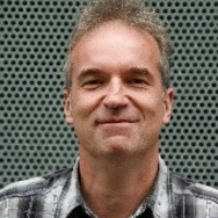
Jens Bliedtner studied
precision engineering at the Friedrich Schiller University in Jena. He wrote
his doctoral thesis in the fields of development of pulsed laser systems and
special methods in macro material processing. Since 2000, Bliedtner has been a
professor at the Ernst Abbe University of Applied Sciences in Jena and the head
of the department production engineering and automation of production
processes. Currently, he is working in the research fields of optical
technology, laser material processing and additive manufacturing.
